![]()
![]()
![]()
![]()

Electron ptychography is a cutting-edge imaging technique that enables us to recover the phase information of scattered electrons, which is typically lost in conventional electron microscopy. In ptychography, we scan a convergent electron probe across the sample in a series of overlapping positions, recording a diffraction pattern at each point. The overlap between probe positions introduces redundancy in the collected data, which we exploit using iterative algorithms to solve the inverse problem and to computationally reconstruct both the electron probe and the sample.
A particularly powerful approach is multislice electron ptychography (MEP), where we explicitly model the electron sample interaction as a sequence of propagation and scattering steps through multiple thin slices of the sample. This multislice framework allows us to accurately account for multiple scattering events, making it especially suitable for thicker or more complex specimens.
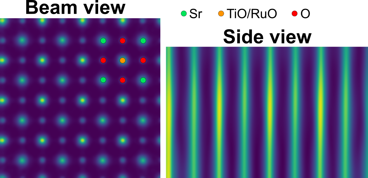
MEP provides us with significantly more information about the sample than standard imaging techniques. Notably, MEP allows us to simultaneously image both light and heavy elements with high contrast, which is challenging for conventional methods. Furthermore, MEP can achieve spatial resolutions beyond the conventional diffraction limit, effectively making it a super-resolution technique. Since the reconstruction incorporates the three-dimensional propagation of electrons, the resulting reconstructions are not simple 2D projections but inherently contain 3D structural information.
These advantages make electron ptychography, and MEP in particular, highly effective for investigating extended crystal defects such as grain boundaries, dislocations, and interfaces. These defects often exhibit irregular and complex structures that require accurate, high-resolution imaging. By applying MEP, we are able to study these extended defects in unprecedented detail, which is particularly valuable for advancing our understanding of energy and quantum materials.
Copyright © ATEM 2026
Last update: Feb 17, 2026