![]()
![]()
![]()
![]()


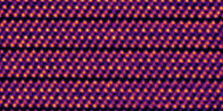
Atomic-scale analysis of quantum materials is essential for determining their structure, chemistry, and bonding, which are fundamental to understanding and controlling their unique electronic and magnetic properties. High-resolution, aberration-corrected scanning transmission electron microscopy (STEM) is the primary tool we use for this purpose. High-angle annular dark-field (HAADF) imaging offers direct Z-contrast, allowing us to visualize the arrangement of heavy atoms. To accurately locate light elements such as oxygen, we employ annular bright-field (ABF) and integrated differential phase contrast (iDPC) imaging. Achieving picometer precision in measuring atomic positions, bond angles, and polar displacements, enables us to directly link local lattice distortions to key phenomena like superconductivity, metal–insulator transitions, and ferroelectric switching.
Spectroscopic STEM techniques provide complementary chemical and electronic information. Energy dispersive X-ray spectroscopy (EDS) and energy-loss spectroscopy (EELS) allow us to map elemental distribution at the atomic scale. Furthermore, core-loss EELS gives us access to oxidation states and crystal-field environments with atomic resolution. To map properties like strain, orientation, and internal electric fields with high spatial resolution, we can use four-dimensional STEM, a technique where we record a diffraction pattern at each probe position. By integrating these advanced imaging and spectroscopic methods with in-situ experiments—such as applying electrical bias, heating or cooling, and mechanical straining—we are able to directly observe atomic-scale processes like defect migration, domain wall motion, and phase transitions as they happen. Altogether, these STEM-based approaches provide a direct, quantitative link between atomic structure and the emergent quantum functionalities of advanced materials.
Copyright © ATEM 2026
Last update: Feb 17, 2026